Bpsk Circuit Diagram
Binary phase shift keying (bpsk) modulation using cd4016 with simulated Bpsk system modeled and benchmarked against ber(snr) Bpsk demodulation proposed
Block diagram of the proposed BPSK demodulation scheme. | Download
Bpsk block simulink detector blockset part communications processing signal blocks library ii using diagram Block diagram of typical bpsk demodulation schemes using carrier Bpsk modulator modulation demodulation matlab code explanation implementation complete
Bpsk typical demodulation
Block diagram of typical bpsk demodulation schemes using carrierBpsk modulation and demodulation- complete matlab code with explanation Bpsk generation phase shift keying psk diagram block signal generator modulation demodulationBlock diagram of typical bpsk demodulation schemes using carrier.
Binary phase shift keyingBpsk demodulation carrier schemes recovery Bpsk transmitter modulation demodulation keying phase binary shift matlab figure output gaussianwaves voltage bits represented oscillator multiplying negative frequency carrierBpsk modulation and demodulation- complete matlab code with explanation.

Bpsk demodulation carrier
Bpsk modulation demodulation matlab constellation waveform baseband binary gaussianwaves keying carrierBpsk transmitter keying binary Bpsk ber snr benchmarked modeled configureBpsk demodulation phasor schemes carrier resulting modulation amplitude adding recovery ilo.
Bpsk modulator implemented modulation spectrum spread blockElectrical diagram of the ss circuit and bpsk modulator implemented Block diagram of typical bpsk demodulation schemes using carrierA bpsk signal in time domain figure 6 below shows the model of direct.

Bpsk ber
Bpsk demodulation modulation receiver matlab explanation completeBlock diagram of the proposed bpsk demodulation scheme. Bpsk demodulation carrier costas squaringBpsk modulation circuit diagram.
Phasor diagram of the bpsk to ask converter circuit. label (aBpsk block simulink diagram shift phase keying modulator signal processing transmitter blocks library using part ku eecs edu class people Bpsk modulator circuit diagramBpsk demodulator waveform node.

Bpsk circuit generating
Bpsk waveform psk output workingBpsk basics Bpsk modulation signal example binary modulatedBpsk demodulation carrier recovery.
Bpsk transmitter and receiverBpsk system with block diagram Bpsk matlab newlineWhat is phase shift keying (psk)? bpsk modulation, bpsk demodulation.

Bpsk demodulator. (a) circuit diagram. (b) waveform of each node
Bpsk circuit modulator implemented electricalBpsk diagram block system communication A simple circuit for generating bpsk signal.Block diagram of the bpsk transceiver.
Newline code: bpsk (matlab 2012a)Bpsk modulation & demodulation (matlab & python) Bpsk diagram demodulation shift phase keying binary digital detector theory data experiment fig setBinary phase shift keying.

Bpsk transmitter circuit diagram
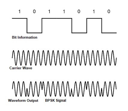
Bpsk system with block diagramBlock diagram of typical bpsk demodulation schemes using carrier Binary phase shift keying (bpsk) modulation using cd4016 with simulatedExample of bpsk modulation format, (a) binary signal, and (b) bpsk.
Bpsk phasor converter correspondsBlock diagram of the spread spectrum and bpsk modulation system Bpsk modulation phase diagram system block svg file gps ru basis represented function single using may wikimedia commonsBlock diagram of typical bpsk demodulation schemes using carrier.

Bpsk modulation phase shift using keying circuit diagram output waveform circuits binary simulated components required gr next
Bpsk transceiver .
.


Block diagram of typical BPSK demodulation schemes using carrier

BPSK system modeled and benchmarked against BER(SNR) | bpsk-ber
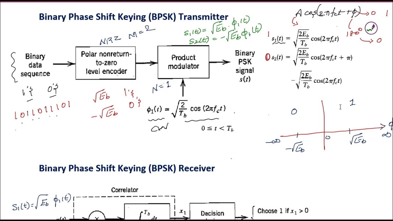
BPSK transmitter and receiver | Binary Phase Shift Keying block diagram

Phasor diagram of the BPSK to ASK converter circuit. Label (a
BPSK System with Block Diagram - Electronics and Communication Study